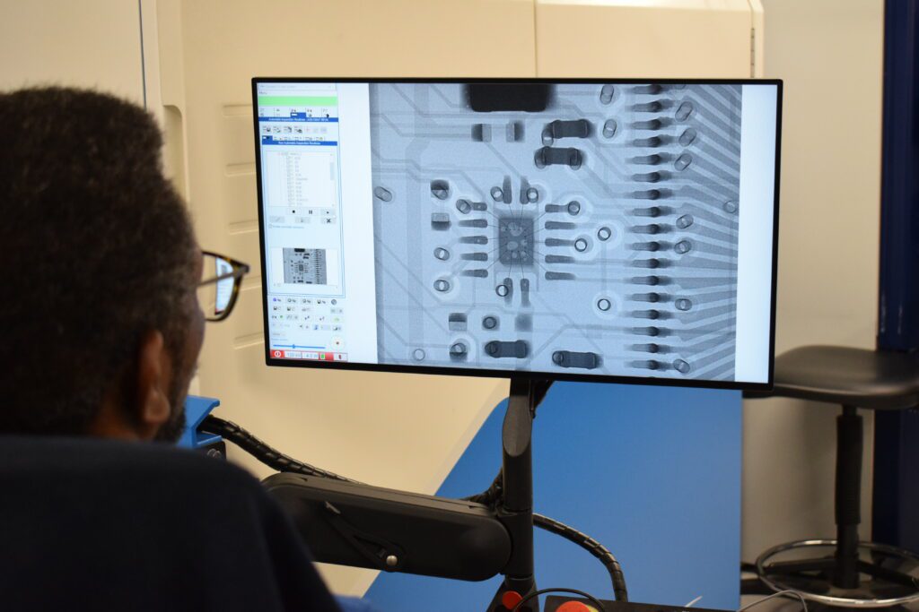
X-Ray Testing
At Active-PCB Solutions, we are committed to delivering the highest quality standards for Printed Circuit Boards (PCBs) by incorporating advanced inspection and testing methods. One of the most crucial steps in our quality assurance process is X-Ray Testing of PBCs.
This powerful, non-destructive inspection method allows us to detect hidden defects in PCBs, ensuring reliability, performance, and longevity in all of our products.
X-Ray Testing of PCBs | Active-PCB Solutions
In modern electronic devices, complex PCBs and micro-components have become the norm. With the rise of Surface Mount Technology (SMT) and components like BGAs (Ball Grid Arrays) and QFNs (Quad Flat No-Lead) packages, which conceal critical connections beneath the surface, traditional visual inspection methods are no longer sufficient for ensuring flawless PCB assembly.
X-Ray Testing enables us to see inside and through even the smallest of components, identifying issues that are invisible to other forms of inspection.
Key Benefits of X-Ray Testing for PCB Assembly
- Defect Detection in Hidden Connections: X-Ray Testing for PCBs is essential for identifying issues such as solder joint defects, misalignment, bridging, and voids in hidden or embedded connections.
- Non-Destructive Testing: Unlike destructive testing methods, this type of testing preserves the integrity of the PCB, allowing us to analyse components without compromising their structure.
- Reduced Risk of Field Failure: Identifying potential issues early in the production cycle allows us to address them before products are assembled, reducing the risk of field failures and increasing customer satisfaction.

Common PCB Defects Detected by X-Ray Testing
Our advanced X-Ray Testing capabilities allow us to detect a wide range of potential issues with printed circuit boards. Such issues might include:
- Solder Joint Voids: Air gaps or bubbles in solder joints that can lead to weak connections and eventual failure.
- BGA and QFN Defects: Misalignments, open connections, or shorts beneath surface-mounted components.
- Delamination and Cracking: Structural issues within the PCB layers that could impact performance over time.
- Component Misalignment: Ensures components are accurately positioned according to design specifications.
Our X-Ray Testing Capabilities
At Active-PCB Solutions, we use cutting-edge Nordson-Dage Quadra 3 and Nordson-Dage XD7600NT X-Ray equipment which is capable of high-resolution imaging, enabling our experts to inspect intricate PCB assemblies and complex, multilayer designs.
We can detect hidden manufacturing internal structures and solder connection defects, checking every layer of the PCB without any risk of damage. With flexible magnification our X-Ray systems provide a thorough analysis, helping to ensure the safety and functionality of each PCB before it reaches our customers.
Partner with Active-PCB Solutions for Reliable PCB Quality
By choosing Active-PCB Solutions, you partner with a team that values quality, innovation, and customer satisfaction. Our rigorous X-Ray Testing process is part of our commitment to excellence in every PCB we deliver. Whether your needs are in high-reliability sectors like aerospace or consumer electronics, we are here to provide high-quality PCBs that meet your exacting standards.
For more information on PCB testing, or to discuss your PCB needs, contact us today. Our experienced team is ready to support your project with industry-leading solutions for robust, reliable PCBs.