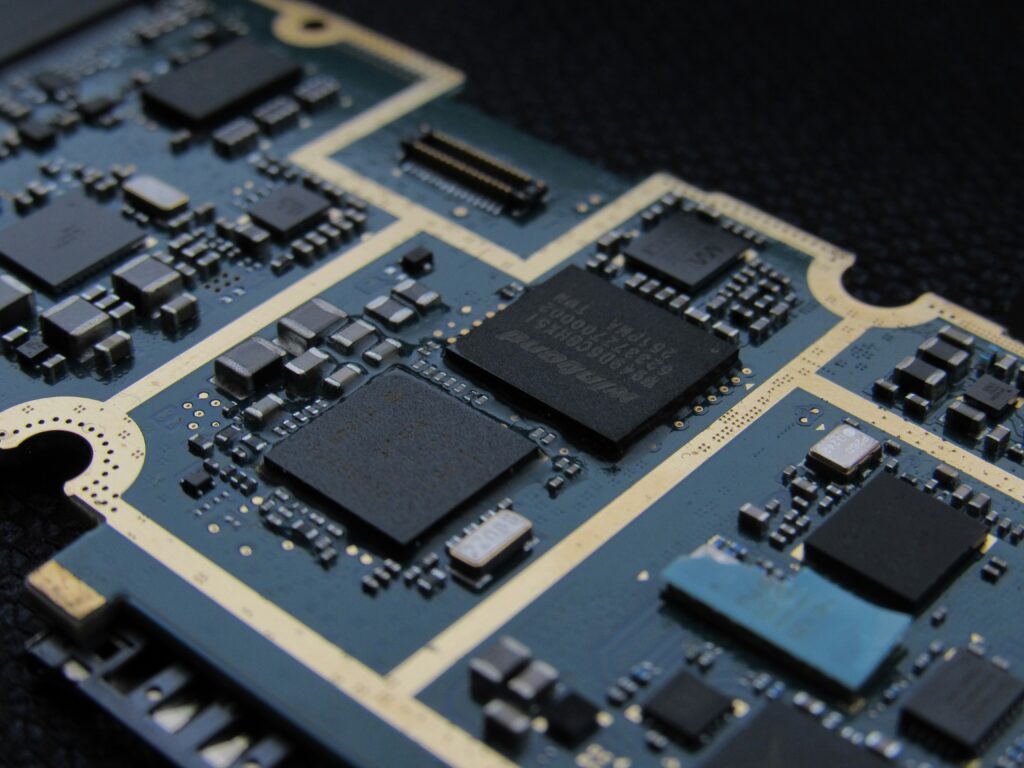
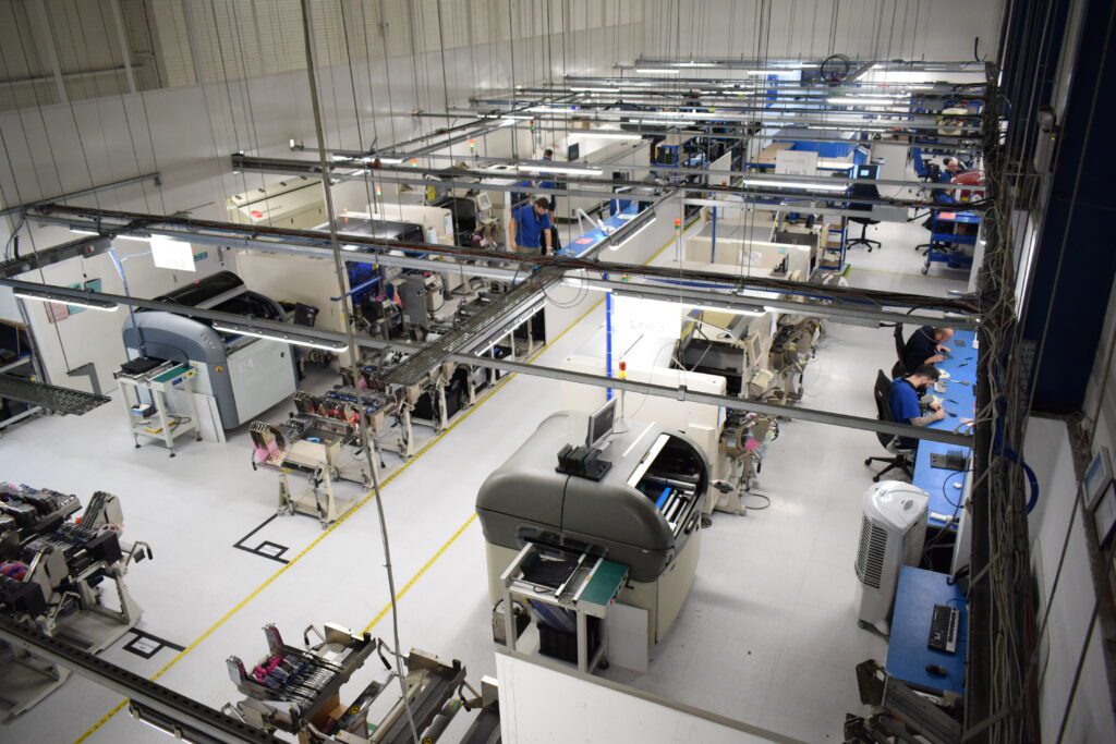
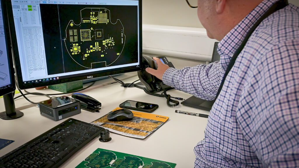
At Active-PCB Solutions we manage a wide range of HDI (High-Density Interconnect) PCBs for our clients. Whether you know it or not, you’re likely carrying an HDI PCB right now; these compact, high-performance boards are at the heart of nearly every smartphone, tablet, and computer, including the one you’re using to read this article.
What Makes HDI PCBs Special?
High-Density Interconnect PCBs have a very high density of circuit connections. To achieve HDI, the PCB has to have extremely small PCB vias and fine traces.
- Microvias:
- Small vias with diameters ≤ 150 µm (6 mils) allow for higher component density.
- Types of Vias:
- Blind Vias: Connect outer layers to inner layers.
- Buried Vias: Connect internal layers without surface exposure.
- Stacked Vias: Vertically aligned microvias across layers.
- Staggered Vias: Offset microvias for flexible routing.
- Track Widths and Spacing:
- Typically ≤ 75 µm (3 mils), enabling precise, compact designs.
- Layer Structure:
- Build-up layers with thin dielectrics ensure high interconnect density.
- Sequential lamination processes allow for complex multi-layer stacking.
Cost Efficiency and Reliability
Advances in technology have significantly reduced the cost of HDI PCBs, making them accessible for a wide range of applications.
But how reliable are they?
Think about your smartphone; it’s a testament to the durability and dependability of HDI PCBs. These boards are designed to handle the huge demands of modern technology seamlessly.
HDI in Everyday Life
From the smartphone or computer in your hands to the AI answering your questions, HDI PCBs power the signals between components that drive innovation. They are the backbone of modern technology, enabling the processing power and connectivity we rely on daily.
Why Do We Need HDI PCBs?
High-Density Interconnect (HDI) PCBs are critical to modern electronics for several reasons, all tied to the growing demand for smaller, faster, and more efficient devices.
Here’s why HDI technology is essential:

1. Miniaturisation
- Compact Designs: As devices like smartphones, wearables, and IoT gadgets shrink in size, PCBs must also become smaller without sacrificing performance.
- More Components in Less Space: HDI PCBs use microvias, thin tracks, and high-density routing to fit more components in compact spaces.
2. Improved Performance
- Signal Integrity: Shorter signal paths and reduced parasitic capacitance/inductance in HDI PCBs improve electrical performance, especially in high-speed and high-frequency applications.
- Reduced Crosstalk: Smaller feature sizes and advanced routing reduce interference between signals.
3. Increased Functionality
- Layer Density: HDI PCBs can have many more layers (up to 100+), enabling complex circuits for advanced functionalities.
- Via-in-Pad Technology: This allows components to sit directly on vias, optimizing space and enhancing thermal performance.
4. Essential for Modern Devices
- Consumer Electronics: Smartphones, tablets, laptops, and smartwatches require HDI PCBs for their compact, high-performance designs.
- AI and Data Processing: HDI boards enable faster signal processing, critical for AI models, servers, and data centers.
- Automotive and Aerospace: The need for lightweight, compact, and reliable PCBs is vital in autonomous vehicles, avionics, and space technology.
5. Cost Efficiency in the Long Run
- While initial HDI manufacturing costs are higher, the ability to consolidate functionality into fewer boards and improve device reliability reduces overall costs for manufacturers and users.
- Material Efficiency: Smaller boards mean less raw material is used.
- Energy Savings: HDI PCBs often contribute to more energy-efficient devices, helping reduce the carbon footprint.
In short, HDI PCBs really are are the backbone of modern technology, enabling manufacturers to meet the demand for smaller, faster, and smarter devices while delivering excellent performance and reliability.
At Active-PCB, our world-class PCB manufacturers can produce the most complex HDI PCBs – up to 100 layers! Whatever your needs, we’re here to deliver quality and reliability. Contact us to find out more!


