PCB Testing is a crucial step in the manufacturing process of printed circuit boards (PCBs). Whether you’re producing small-scale prototypes or doing large-scale mass production runs, testing ensures that your PCBs meet quality standards and function as intended.
Without thorough testing, even the smallest defect can lead to device malfunction, causing delays, increased costs, or worse; product failures in the field and disappointment from the end user.
Here we’ll run through the different methods of PCB testing, including Automatic Optical Inspection (AOI), X-ray inspection, and functional testing, to help you understand the best way to ensure the quality of your PCBs.
Why is PCB Testing Important?
Before diving into the specifics of each method, it’s probably useful to think about why PCB testing is critical.
- Quality Assurance: Testing identifies defects such as poor solder joints, misaligned components, or shorts and opens, ensuring that the PCB is free of manufacturing defects.
- Reliability: By catching issues early, you reduce the risk of field failures, improving the reliability of your products which means higher customer satisfaction.
- Cost Reduction: Early detection of any faults in boards minimises rework and scrap costs, ensuring that only functional PCBs move forward in the production process.
Here are some of the most commonly used methods for testing PCBs.
1. Automated Optical Inspection (AOI)
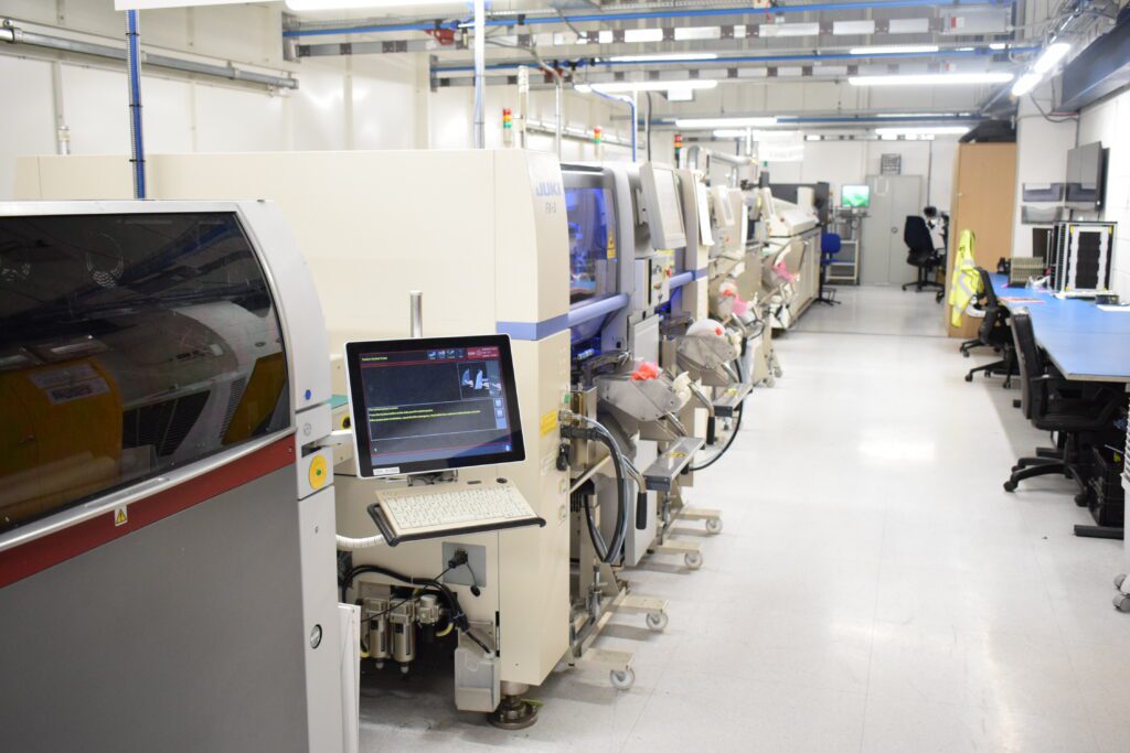
Automated Optical Inspection (AOI) is a widely used technique in PCB testing, especially for detecting defects during assembly. This method uses high-resolution cameras to capture images of the PCB and compare them against a predefined set of standards. At Active-PCB, we use new 3D AOI Koh Young Technology in partnership with Altus Group, who provide the K-Smart software system to identify any defects.
Key Advantages of AOI:
- Non-contact: AOI is a non-invasive method, meaning it does not physically touch the PCB during inspection, minimizing the risk of damage.
- Speed: The process is quick, allowing for rapid inspection, making it ideal for high-volume production. At Active-PCB, we have AOI connected to the SMT line so that all PCBs can be tested in real time and the line stopped if something is found to be wrong.
- Versatility: AOI can detect a range of defects, including missing components, incorrect polarity, and soldering issues.
When to Use AOI: AOI is particularly effective for inspecting surface-mounted technology (SMT) components. It is often used after the soldering process to ensure that each component is properly placed and soldered onto the board. While it’s excellent for visual checks, AOI cannot inspect internal features like solder joint quality within Ball Grid Arrays (BGAs), which is where X-ray inspection comes into play.
2. X-ray Inspection
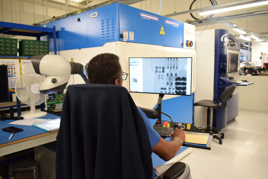
X-ray inspection is another powerful tool for testing PCBs, especially when dealing with complex boards and tiny components that may not even be visible to the naked eye. This method uses X-rays to penetrate the PCB, creating an image that reveals hidden features such as internal solder joints and connections.
Key Advantages of X-ray PCB Inspection:
- Non-destructive PCB Testing: Like AOI, X-ray inspection is non-destructive, allowing you to inspect internal structures without touching or damaging the PCB.
- Detailed Internal View: It can detect issues like voids in solder joints, shorts, opens, and internal layer misalignments, which are invisible to other inspection methods.
- Ideal for BGAs: X-ray is especially useful for inspecting BGAs and other components where the solder joints are hidden beneath the package.
When to Use X-ray Inspection: X-ray inspection is typically used for more advanced testing needs, such as when working with multilayer PCBs or assemblies that use BGAs, micro BGAs, or flip chips. It is often employed as a secondary method to complement AOI, especially when visual inspection cannot provide enough detail.
3. Functional Testing
Functional testing is a critical phase in PCB testing, as it evaluates whether the PCB performs according to its intended purpose. Unlike AOI or X-ray, which focus on visual and structural integrity, functional testing ensures that the board operates correctly under real-world conditions.
Key Advantages of Functional Testing:
- Application-Specific: Functional testing is tailored to the specific application of the PCB, ensuring it meets performance standards.
- Holistic Check: It tests the complete board functionality, including power up, signal transmission, and communication with other parts of the system.
- Customizable: Functional tests can be customized based on the requirements of the product, making it flexible for different PCB designs.
When to Use Functional Testing: Functional testing is typically the final step before a PCB moves to production. It is most effective after the board has passed AOI and X-ray inspections, confirming that the board can handle its electrical load, communication protocols, and overall functionality.
4. In-Circuit Testing (ICT)
In-circuit testing (ICT) is another method used for testing PCBs, primarily to check the integrity of individual components and electrical pathways on the board. ICT involves placing the PCB into a fixture with probes that contact the test points on the PCB, allowing for detailed checks of each component.
Key Advantages of ICT:
- Comprehensive: ICT can verify the functionality of individual components, as well as the connections between them, providing detailed insights into component-level issues.
- High Fault Coverage: It can detect issues such as shorts, opens, and value errors for passive components, making it ideal for identifying assembly defects.
When to Use ICT: ICT is most effective for high-volume production, where consistent quality needs to be maintained across a large number of units. However, it requires custom test fixtures and programming, making it less suitable for small runs or prototype testing.
5. Flying Probe PCB Testing
Flying probe testing is an alternative to ICT, particularly suited for small batch sizes or prototypes where building a custom test fixture isn’t cost-effective. In this method, a set of probes move across the PCB, making contact with various test points to measure electrical characteristics like resistance, capacitance, and inductance.
Key Advantages of Flying Probe Testing:
- Cost-Effective for Prototyping: Since it does not require a custom fixture, it’s ideal for testing prototypes or low-volume production.
- Flexibility: It can be easily adapted to different PCB designs without needing extensive setup.
When to Use Flying Probe Testing: Flying probe testing is best used during the early stages of development or for short-run manufacturing. It is slower than ICT but offers flexibility and lower setup costs, making it perfect for small-scale or prototype testing.
Choosing the Right PCB Testing Method
Selecting the right PCB testing method depends on the complexity of your board, the production volume, and the nature of defects you are trying to detect. Here’s a quick recap to guide your decision:
- AOI: Best for detecting visual defects in high-volume production, particularly for SMT components.
- X-ray: Ideal for inspecting hidden connections, like those in BGAs, and for complex multilayer boards.
- Functional Testing: Ensures the PCB performs as intended under real-world conditions and is typically the final step before production.
- ICT: Suitable for detailed component-level testing in large-scale production runs.
- Flying Probe Testing: Cost-effective and flexible for prototype testing and low-volume runs.
By integrating a combination of these testing methods, Active-PCB Solutions can ensure that your PCBs meet the highest standards of quality and reliability. Whether you are producing a small batch of prototypes or gearing up for mass production, thorough PCB testing is your key to success.
Let us help you ensure that every board you produce is a perfect fit for its intended application; contact us now to speak with our experts.

